- 您现在的位置:买卖IC网 > Sheet目录2005 > LTC2242IUP-10#PBF (Linear Technology)IC ADC 10BIT 250MSPS 64-QFN
LTC2242-10
19
224210fd
applicaTions inForMaTion
Maximum and Minimum Encode Rates
ThemaximumencoderatefortheLTC2242-10is250Msps.
For the ADC to operate properly, the encode signal should
have a 50% (±5%) duty cycle. Each half cycle must have
at least 1.9ns for the ADC internal circuitry to have enough
settling time for proper operation. Achieving a precise
50% duty cycle is easy with differential sinusoidal drive
using a transformer or using symmetric differential logic
such as PECL or LVDS.
An optional clock duty cycle stabilizer circuit can be used if
the input clock has a non 50% duty cycle. This circuit uses
the rising edge of the ENC+ pin to sample the analog input.
The falling edge of ENC+ is ignored and the internal falling
edge is generated by a phase-locked loop. The input clock
duty cycle can vary from 40% to 60% and the clock duty
cycle stabilizer will maintain a constant 50% internal duty
cycle. If the clock is turned off for a long period of time,
the duty cycle stabilizer circuit will require one hundred
clock cycles for the PLL to lock onto the input clock. To
use the clock duty cycle stabilizer, the MODE pin should be
connected to 1/3VDD or 2/3VDD using external resistors.
ThelowerlimitoftheLTC2242-10samplerateisdetermined
by droop of the sample-and-hold circuits. The pipelined
architecture of this ADC relies on storing analog signals on
small valued capacitors. Junction leakage will discharge
thecapacitors.Thespecifiedminimumoperatingfrequency
for the LTC2242-10 is 1Msps.
DIGITAL OUTPUTS
Table 1 shows the relationship between the analog input
voltage, the digital data bits, and the overflow bit.
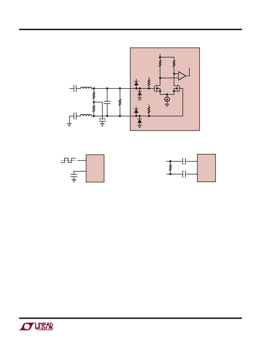
Figure 11. Transformer Driven ENC+/ENC–
Figure 12a. Single-Ended ENC Drive,
Not Recommended for Low Jitter
Figure 12b. ENC Drive Using LVDS
VDD
LTC2242-10
224210 F11
VDD
ENC–
ENC+
1.5V BIAS
0.1μF
T1
MA/COM
ETC1-1-13
CLOCK
INPUT
100Ω
8.2pF
0.1μF
50Ω
50Ω
4.8k
TO INTERNAL
ADC CIRCUITS
224210 F12a
ENC–
1.5V
VTHRESHOLD = 1.5V
ENC+
0.1μF
LTC2242-10
224210 F12b
ENC–
ENC+
LVDS
CLOCK
100Ω
0.1μF
LTC2242-10
0.1μF
发布紧急采购,3分钟左右您将得到回复。
相关PDF资料
LTC2245IUH#TRPBF
IC ADC 14BIT 10MSPS 3V 32-QFN
LTC2249IUH#TRPBF
IC ADC 14BIT 80MSPS LP 32-QFN
LTC2251IUH#PBF
IC ADC 10-BIT 125MSPS 3V 32-QFN
LTC2253IUH#TRPBF
IC ADC 12BIT 125MSPS 3V 32-QFN
LTC2255CUH#TRPBF
IC ADC 14BIT 125MSPS 3V 32-QFN
LTC2258IUJ-12#PBF
IC ADC 12BIT 65MSPS 1.8V 40-QFN
LTC2262CUJ-14#TRPBF
IC ADC 14BIT 150MSPS 40-QFN
LTC2262IUJ-12#PBF
IC ADC 12BIT 150MSPS 40-QFN
相关代理商/技术参数
LTC2242IUP-10#TRPBF
功能描述:IC ADC 10BIT 250MSPS 64-QFN RoHS:是 类别:集成电路 (IC) >> 数据采集 - 模数转换器 系列:- 标准包装:1 系列:- 位数:14 采样率(每秒):83k 数据接口:串行,并联 转换器数目:1 功率耗散(最大):95mW 电压电源:双 ± 工作温度:0°C ~ 70°C 安装类型:通孔 封装/外壳:28-DIP(0.600",15.24mm) 供应商设备封装:28-PDIP 包装:管件 输入数目和类型:1 个单端,双极
LTC2242IUP-10-PBF
制造商:LINER 制造商全称:Linear Technology 功能描述:10-Bit, 250Msps ADC
LTC2242IUP-10-TR
制造商:LINER 制造商全称:Linear Technology 功能描述:10-Bit, 250Msps ADC
LTC2242IUP-10-TRPBF
制造商:LINER 制造商全称:Linear Technology 功能描述:10-Bit, 250Msps ADC
LTC2242IUP-12
制造商:Linear Technology 功能描述:ADC Single Pipelined 250Msps 12-bit Parallel/LVDS 64-Pin QFN EP 制造商:Linear Technology 功能描述:MS-ADC/High Speed, 12-bit, 250Msps ADC
LTC2242IUP-12#PBF
制造商:Linear Technology 功能描述:ADC Single Pipelined 250Msps 12-bit Parallel/LVDS 64-Pin QFN EP 制造商:Linear Technology 功能描述:Single ADC Pipelined 250Msps 12-bit Parallel/LVDS 64-Pin QFN EP 制造商:Linear Technology 功能描述:IC ADC 12BIT 250MSPS 64-QFN 制造商:Linear Technology 功能描述:A/D Converter (A-D) IC 制造商:Linear Technology 功能描述:IC, ADC, 12BIT, 250MSPS, QFN-64, Resolution (Bits):12bit, Sampling Rate:250MSPS, Supply Voltage Type:Single, Supply Voltage Min:2.375V, Supply Voltage Max:2.625V, Supply Current:285mA, Digital IC Case Style:QFN, No. of Pins:64 , RoHS Compliant: Yes 制造商:Linear Technology 功能描述:MS-ADC/High Speed, 12-bit, 250Msps ADC
LTC2242IUP-12#TRPBF
制造商:Linear Technology 功能描述:ADC Single Pipelined 250Msps 12-bit Parallel/LVDS 64-Pin QFN EP T/R 制造商:Linear Technology 功能描述:IC ADC 12BIT 250MSPS 64-QFN
LTC2242UP-10
制造商:LINER 制造商全称:Linear Technology 功能描述:10-Bit, 250Msps ADC